Tapping a Parallel Memory Bus

Serial flash sends data on one line, which makes it easy to read. Parallel memory moves many bits at once across address and data buses, which is faster for the device and much harder for an attacker. It still gives up its secrets with enough channels and care.
When Data Moves on Many Wires
A serial SPI flash is a four-wire conversation, and a cheap clip plus a programmer reads it in minutes. Parallel memory is a different problem: it spreads an address across a dozen or more pins, returns data across eight or sixteen more, and coordinates the whole thing with control signals. That width is a performance choice, not a security one, but it has a security side effect, because capturing it is far more work than reading a serial part.
To read a parallel bus live you have to capture the address lines and the data lines at the same instant, then line them up to know which address produced which data. A 16-bit-wide flash with a 20-bit address is over thirty signals before control lines, far past a four-channel hobby analyzer, and the timing is unforgiving too: the data is valid only during a narrow window relative to the control strobes, so the capture has to be both wide and fast. This is the wall that stops casual attempts at a parallel bus.
Identify the Parallel Part First
Confirm you are actually looking at parallel memory before committing to the hard path. A part with 40 or more pins, an address bus, a separate data bus, and chip-enable, output-enable, and write-enable control lines is parallel NOR or NAND. The datasheet’s pinout settles it.
# markings and pinout point to a parallel NOR flash
M29F040B  ->  4 Mbit parallel NOR, 32-pin
# A0-A18 address, DQ0-DQ7 data, plus CE#, OE#, WE#
-> 19 address lines + 8 data lines + 3 control = 30 signals to capture live
-> or: remove the chip and read it in a programmer (far simpler)
Thirty signals to capture in sync is the live-tap cost. Seeing that number is usually the moment you start considering whether removing the chip is the smarter move, which it often is.
Live Tap or Desolder?
Two routes recover the firmware, and the choice between them is the whole strategy for a parallel part:
| Factor | Live bus tap | Desolder + programmer |
|---|---|---|
| Channels needed | 30+ in sync (address, data, control) | None; the programmer drives its own bus |
| Coverage | Only addresses read while you watched | Every address, a complete image |
| Timing | Must sample the narrow valid window | Controlled by the programmer |
| Device keeps running | Yes | No, the chip is removed |
| Setup | A finicky 30-probe hookup | Hot-air the chip onto an adapter |
The live tap earns its cost only when you specifically need to watch which addresses the device accesses while running. For simply recovering the firmware, the socketed read wins, and the sections below walk both so the tradeoff is concrete.
The Channel-Count Problem
Capturing this live needs a logic analyzer with enough channels and enough speed to sample every line through the access window. That is a real instrument, not a hobby board, and setting up thirty-plus probe connections on a dense board is finicky and error-prone.
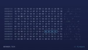
# a high-channel analyzer configured for a parallel capture
sigrok-cli -d fx2lafw --channels A0-A18,DQ0-DQ7,CE,OE,WE \
--config samplerate=24MHz --samples 5M -o capture.srsaved 5M samples across 30 channels to capture.sr # now the hard part: correlate address to data to rebuild the memory map
Even with the capture in hand, the raw samples are not firmware. They are millions of bus transactions that still have to be turned back into an ordered image, which is the next problem.
Correlating Address and Data
The value of a parallel capture is matching the address being driven to the data that comes back during each read. Post-processing walks the capture, samples the data bus on each output-enable strobe, and writes the byte to the address that was present.
# pseudo-reconstruction: on each OE# strobe, record data at the current address
for each falling_edge(OE):
    addr = read_bits(A0..A18)
    data = read_bits(DQ0..DQ7)
image[addr] = datareconstructed 4 Mbit image, 92% of addresses observed # gaps where the CPU never read certain regions during capture
A live capture only ever sees the addresses the device actually read while you watched. Regions the firmware never touched stay blank, so a live tap often yields a partial image, which is another reason the direct read tends to win.
Reading It in a Programmer
More often than not, removing the chip and reading it in a dedicated programmer is easier than tapping a live bus. Hot air and a little practice lift a parallel chip onto an adapter without damage, and a universal programmer that supports the part reads the whole chip over its own controlled bus, no correlation required, the parallel equivalent of dropping a SPI chip into a CH341A.
# read a parallel NOR chip in a universal programmer
minipro -p "M29F040B@DIP32" -r dump.binFound Microchip M29F040B Reading Code... 4.19s Verification OK # complete 512 KB image, every address, no gaps
One command, a complete image, every address present. That is why the socketed read usually beats the live tap: it is faster to set up, it cannot miss a region, and it does not fight the bus timing. The trade is that the device stops running, which matters only if you specifically needed to watch live accesses.
NOR Versus NAND on a Parallel Bus
Knowing which type you have changes the plan. Parallel NOR reads back as a clean linear image, read-and-go. Parallel NAND is messier, because it carries spare areas, ECC bytes, and bad-block markers alongside the data, so a raw dump needs a reader that understands page-and-spare layout, then stripping ECC and reassembling pages before any filesystem appears. The extra step is the same whether you tapped the bus or read the chip.
Estimating the Effort before You Start
A quick estimate keeps you from committing to the hard path needlessly. Count the address and data lines from the datasheet, add the control signals, and compare against your analyzer’s channel count and speed. If the signal count exceeds your gear, or the bus runs faster than you can sample cleanly, the live tap is off the table before you solder a single probe.
# rough feasibility check for a live parallel capture
addr_lines=19; data_lines=8; control=3
channels_needed=$((addr_lines + data_lines + control))   # = 30
echo "need $channels_needed channels at >= 2x bus clock to capture cleanly"need 30 channels at >= 2x bus clock to capture cleanly # a typical 16-channel analyzer cannot do this -> read the chip in a programmer
When the arithmetic says thirty channels and you own sixteen, the decision is made: remove the chip and read it in a programmer. Doing this estimate first turns a frustrating, doomed live-tap attempt into a five-minute calculation that points you at the path that actually works.
What It Reveals, and What Defenders Should Do
The prize is the same as any flash read: the bootloader, the firmware, the configuration, and any secrets stored alongside them. The wider bus changed the effort to get there, not the value of what is there, which is the core point for attacker and defender alike, that a parallel layout is a performance and cost decision that happens to raise the bar for extraction but is not a security control.
So a sensitive firmware image on parallel memory needs the same protections as one on serial flash: encryption with a hardware-held key, and verified boot so a modified image will not run. Betting on the difficulty of tapping a wide bus is betting that an attacker will not simply lift the chip, which they will, because the desolder-and-read shortcut neutralizes the effort entirely. The real defenses are the cryptographic ones that do not depend on how the bytes are wired.
Where This Fits
Assessing how exposed a device’s storage is, parallel or serial, is a core part of a hardware penetration test. If you want a clear read on what your firmware and stored secrets give away, that is the kind of work we do at Berkner Tech.